
Thank you for Subscribing to Semiconductor Review Weekly Brief
× 
Semi Conductor Review Weekly Brief
Be first to read the latest tech news, Industry Leader's Insights, and CIO interviews of medium and large enterprises exclusively from Semi Conductor Review
Heidelberg Instruments has been recognized by Semiconductor Review Magazine as “Top Sustainable Maskless Lithography Solutions - 2025” based on our proprietary methodology, reflecting its position in the industry. This profile has been developed by the Semiconductor Review research and editorial team based on insights from an interview with Steffen Diez, COO.



Heidelberg Instruments
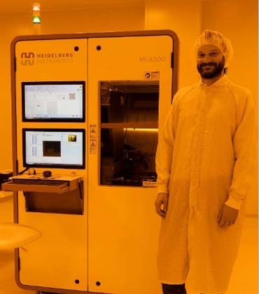 Steffen Diez, COO
Historically, optical lithography exclusively relied on photomasks or reticles, either using a mask aligner or a stepper. Direct writing was first introduced as a method specifically to produce these photomasks, with e-beam lithography being the first direct-write technology in the nineteen-seventies. Direct-write laser lithography was developed since the mid-eighties – again, with the production of photomasks as its core application. From the start, it was obvious that the technique also had great potential for directly writing the pattern on the substrate wafer. However, the throughput of the early direct-write systems was too slow to make this a feasible option for more than the occasional application.
In 2012, this was the starting point for the development of the Heidelberg Instruments’ Maskless Aligner, which was conceptualized as a tool that would revolutionize the way microstructures were created in cleanrooms. “The MLA 150 Maskless Aligner was created to address bottlenecks in multi-user cleanrooms caused by aging mask aligners and time-consuming photomask production. Heidelberg Instruments envisioned a direct-write solution with better performance than a mask aligner—without the delays”, states Dr. Benedikt Stender, Strategic Product Manager MLA 150 system, Heidelberg Instruments. The design specifically addressed all the aspects and solved the problems that had previously deterred users from directly patterning their substrates. It placed a strong emphasis on speed, flexibility, user-friendliness, and accuracy, with a clear view on making it a system that could be used in multi-user facilities and integrated into multi-tool processes. The MLA was released in 2015, celebrating its 10th anniversary in 2025.
Bringing High Speed and Flexibility to Cleanrooms as the New Standard
One of the technical developments that made this possible was the invention and advancement of the DMD™ by Texas Instruments – an array of programmable micro-mirrors. A laser beam is reflected from the mirrors to the substrate, where the pattern is written in a raster, stripe by stripe. The micro-mirror-array (like other spatial light modulators) essentially acts like a “dynamic mask”.
With the combination of the DMD™ and a diode laser, a powerful optical engine was designed for the MLA 150. This meant a significantly higher throughput than other direct write systems, which relied on the combination of acousto-optical devices. In addition, the Maskless Aligner was specifically designed to be easy to operate, so that it could be used comfortably in a multi-user cleanroom. Due to the high speed, the flexibility of the maskless approach was finally available as standard in research and development environments, as well as offering fast turnaround in rapid prototyping and production. Excellent alignment capabilities meant that multi-layer applications as well as mix-and-match applications with other tools yielded extremely precise results. The system allowed the realization of highly complex designs and provided high resolution (at the time of its release that was 1 µm and later, 0.6 µm). As technology advances, the MLA 150 continues to be updated, and today, a write mode is available that enables a minimum feature size of 0.45 µm. An example showing such high-resolution structures is shown in Figure 1
Figure 1
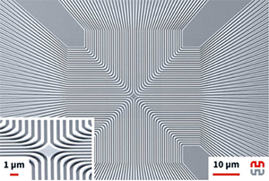
450 nm lines and spaces generated in 300 nm thick AZ MIR photoresist by applying the High-Quality Mode of the MLA 150 with its finest pixel interpolation during exposure.
Source: Heidelberg Instruments Mikrotechnik GmbH
Aside from its flexibility and alignment capabilities, the maskless approach offers additional advantages, ensuring consistent exposure quality even on difficult substrates: the exposure coordinate system can be adjusted to compensate for first layer pattern distortions on the surface, while the real-time autofocus provides constant focus even across height differences, and therefore allows the precise patterning of warped substrates or those with a topography. The MLA 150 offers different exposure modes, two types of autofocus, two laser wavelengths, and is equipped with an environmental chamber with temperature regulation. It is frequently and affectionally referred to as the workhorse in many laboratories.
The Maskless Aligner was released both in a desktop version and the advanced MLA 150 version and swiftly won over the research community. Equally, it became established in prototyping. It is easy to see why – a small change or adaptation in the pattern does not mean a lengthy photomask production process but can be quickly implemented via the software. At the same time, the throughput is high enough to enable small production runs. Looking at the cycle time as a whole, the Maskless Aligner even outpaces the conventional mask aligner. These advantages also meant that industrial users were interested in the new technique from the beginning, especially for R&D or low-volume production, such as customized electronics (Figure 2 shows a packaging demonstrator written by the MLA 300 as an example), sensors, or legacy products.
Figure 2
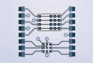
Shown here is a packaging demonstrator, a simulation of chip misalignment in chrome with connector traces exposed by MLA 300 in negative resist.
Source: Heidelberg Instruments Mikrotechnik GmbH
Scaling Maskless Lithography for Industrial Throughput and Advanced Packaging
The industrial version of the Mask Aligner had been planned since the inception of the MLA 150. Listening to feedback and based on the requirements and experience of keen industrial MLA users, Heidelberg Instruments developed the MLA 300, based on the same technology, but offering a larger exposure area as well as higher throughput and equipped with full automation for handling substrates. The system was released in 2019 and featured a unique optical module. A wide choice of load ports and handlers means that it can be precisely tailored to a user’s cleanroom and demands. Applications involving serialization, or thick resists (like MEMS) have benefited hugely from the capabilities of the MLA 300. This includes advanced packaging, specifically fan-out wafer level packaging (FOWLP), and probe cards.
The Maskless Aligner has been a game changer for microstructuring, no matter what type of facility and application. It is one of Heidelberg Instruments’ most successful product lines but has also caused a paradigm shift in microlithography in general, paving the way for direct writing on the substrate as an established technology.
While mask-based lithography processes will always be indispensable in many major industrial areas, direct writing has become a routine technique in academic and industrial research as well as low-volume production, facilitating and streamlining many production and development processes.
This content is copyright protected
However, if you would like to share the information in this article, you may use the link below: