


Thank you for Subscribing to Semiconductor Review Weekly Brief
× 
Semi Conductor Review Weekly Brief
Be first to read the latest tech news, Industry Leader's Insights, and CIO interviews of medium and large enterprises exclusively from Semi Conductor Review
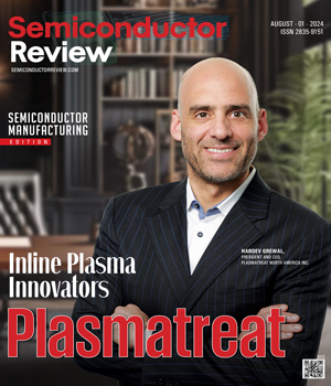
Plasmatreat has been recognized by Semiconductor Review Magazine as “Top 10 Semiconductor Manufacturing Solutions Providers - 2024” based on our proprietary methodology, reflecting its position in the industry. This profile has been developed by the Semiconductor Review research and editorial team based on insights from an interview with HARDEV GREWAL, PRESIDENT AND CEO, PLASMATREAT NORTH AMERICA INC..


 HARDEV GREWAL, PRESIDENT AND CEO, PLASMATREAT NORTH AMERICA INC.
For years, chip packaging has relied on vacuum-based plasma processes. The shrinking component size in wafer processing creates new challenges. These components need treatment during the manufacturing process to maintain efficiency. Traditional cleaning methods, such as batch processing in low-pressure plasma systems or surface treatment with harmful chemicals have their limitations. The primary hurdles are not only the cost of implementation but the inability to deploy these methods in assembly lines and their environmental impact.
Plasmatreat’s Openair-Plasma® technology seamlessly lends itself to an inline process. It perfectly slots into any manufacturer’s assembly line to facilitate atmospheric plasma treatment between steps, improving surface quality and eliminating uncertainties of cross-contamination and recontamination. The microfine cleaning system is ideal for highly sensitive electronic components, replacing the vacuum chamber and wet chemical cleaning in the chip packaging process efficiently and cost-effectively.
“Our technology has a small carbon footprint, reduced capital expenditure and lower operating expenses as it relies only on electricity, clean compressed air and forming gas,” says Hardev Grewal, president and CEO of Plasmatreat North America.
Generating Plasma Akin to the Northern Lights
The plasma is generated by ionizing clean, compressed air through electrical discharge, similar to the natural phenomenon of the northern lights. A plasma jet system operating at atmospheric pressure is used for the pretreatment of various materials. It includes a generator and an industry 4.0-ready plasma control unit, allowing the modification of plasma parameters to optimize the process for specific applications. Critical properties, such as power and flow rate, are continuously monitored during processing. The plasma is generated by an arc discharge occurring upstream of the plasma jet nozzle and involves a working gas. The activated air cleans and functionalizes surfaces, removing all organic micro-contaminants.
Unlike vacuum plasma processes, it allows for area-selective treatment, a capability that facilitates targeted surface treatment during the manufacturing cycle. Whether applying adhesives or conducting thermal compression bonding in advanced semiconductor packaging following the plasma treatment, area selection ensures surfaces are cleaned and activated precisely where required. This targeted approach minimizes energy consumption, reduces chemical use and optimizes efficiency.
The REDOX-Tool
Over the past few years, Plasmatreat has developed plasma processes that can remove metal oxide layers prior to chip bonding. The miniaturization of electronic components means even the slightest oxides can hinder electrical connectivity. Eliminating oxide layers effectively is essential to optimize performance and efficiency in modern electronic devices.
Using its Openair-Plasma® technology, Plasmatreat developed the REDOX-Tool to address the needs of the electronics industry. The tool enables the removal of oxide layers during the production of printed circuit boards or power modules without using flux. Designed as a tunnel solution, the system can also be used in processes that require oxide removal from metal surfaces, for example, before sintering, die bonding, wire bonding and flux-free thermocompression bonding.
A Breakthrough in Atmospheric CVD Coatings
The solution proved so successful that it has been implemented globally by chip manufacturers. Plasmatreat proceeded to present the system to the electronics world at Productronica in November of 2023, where it garnered interest from many other companies in the chip packaging and semiconductor sectors and received the Global SMTA Award in the field of plasma systems.
-
Our technology has a small carbon footprint, reduced capital expenditure and lower operating expenses as it relies only on electricity, clean compressed air and forming gas
A Breakthrough in Atmospheric CVD Coatings
Openair-Plasma’s® ability to apply nano-thick, solvent-free, plasma polymer coatings to a selected surface is generating considerable industry interest. The process is comparable to traditional vacuum plasma-enhanced chemical vapor deposition (PECVD) but in atmospheric conditions. Characteristics of the coating can be determined by a precursor fluid that is vaporized within the plasma. Typical coating properties are hydrophobic, hydrophilic, isolation barriers, moisture barriers, corrosion protection layers and bonding layers.
Of specific note is its capability to apply a dielectric barrier coating on electronic devices. This is a significant breakthrough in the protection of electronic components, as it provides anti-corrosion protection on batteries and flexible electronics. Typically, electronic components are protected by applying a conformal coating over printed circuits. Plasmatreat’s dielectric barrier coating method has significantly enhanced this by using CVD combined with area selection to enable the selective application of nanocoating in specific areas of small electronic devices, such as those used in advanced AR and VR technologies.
Plasmatreat has invested heavily in educating the market on the capabilities and benefits of these coatings. Recent demonstrations of the capability of advanced coatings in an atmospheric environment have impressed seasoned semiconductor professionals. This breakthrough has sparked immense excitement within the industry. It is a pivotal advancement as the company prepares to introduce this technology across a wide range of applications.
Customizable and Modular Plasma Systems
Continuous innovation is part of the company ethos. It has enhanced its equipment to be Industry 4.0-ready, incorporating detailed process monitoring capabilities, like the ability to measure plasma density at treatment areas and ensure precise quality controls. Such capabilities are crucial for critical applications in industries like aerospace, automotive and medical devices, where reliability and assurance are paramount.
One significant advantage of atmospheric plasma technology over traditional low-pressure plasma equipment is its simplified operational requirements.
Low-pressure systems necessitate auxiliary equipment such as vacuum pumps and complex subfloor supply and abatement systems. But Openair-Plasma® systems are a streamlined design of smaller, modular machines with fewer components and eliminate the need for handling hazardous gases or toxic chemicals. This results in enhanced operational efficiency and promotes a safer and more environmentally friendly ecosystem.
For clients who prefer not to invest in or operate machines from external suppliers, Plasmatreat offers plasma treatment as a service. Customers can send their parts to the company for treatment by trained professionals and prompt return.
“Our solution is like a Lego set because we can customize how our clients want to use it, and the equipment can easily be integrated into their manufacturing line,” says Grewal.
Operational efficiency is an ever-present priority, especially in inline production environments where speed is critical. Tools are designed to be operator- and maintenance-friendly. Through a quick connect feature, operators can swiftly exchange either a nozzle head or an entire jet in under a minute, minimizing downtime on the production line. Unparalleled versatility with modular configurations enables the seamless transition from treating metal surfaces to accommodating thermally or electrically sensitive parts.
This flexible approach, featuring interchangeable components and parts, has garnered strong industry acclaim. Unlike competitors who require machine returns for repairs that can take up to or more than 24 hours, Plasmatreat’s maintenance, whether preventive or corrective, typically takes only one to two minutes, ensuring continuous and efficient operations.
Our solution is like a lego set because we can customize how our clients want to use it, and the equipment can easily be integrated into their manufacturing line
For clients who prefer not to invest in or operate machines from external suppliers, Plasmatreat offers plasma treatment as a service. Customers can send their parts to the company for treatment by trained professionals and prompt return.
A Global Strategy for Customer-Centric Innovation
Customer-centricity is the backbone of Plasmatreat’s solutions, supported by a diverse team of experts from various industries. Leveraging their collective experience, the company harnesses extensive industry knowledge to meet the diverse needs of clients across different sectors. Its North American operations are supported by 40 professionals who operate a dedicated R&D center in Silicon Valley focused on high-tech product development and an applications lab in the Chicago area specializing in automotive and white goods industries.
Plasmatreat has also established operations in more than 24 countries through labs strategically located near key semiconductor and microelectronics manufacturing hubs. Understanding the importance of customer proximity facilitates demonstrations and trials, a critical aspect of its service.
The current focus involves deploying new technologies, such as the REDOX-Tool and other advanced equipment, to all global lab locations. The initiative aims to showcase these capabilities directly to customers and demonstrate its market-leading innovations beyond the United States. Customer service is available 24/7 across various countries in native languages; a significant advantage that reinforces the company’s commitment to meeting diverse client needs anywhere in the world.
Regarded within the semiconductor and electronics market as a global innovative leader, Plasmatreat is ushering in a new age of plasma-enabled surface activation that is setting the stage for a new status quo.
| Share this Article:Tweet
|
Company
Plasmatreat
Management
HARDEV GREWAL, PRESIDENT AND CEO, PLASMATREAT NORTH AMERICA INC.
Description
Plasmatreat is an innovator in atmospheric plasma technology, transforming semiconductor and electronics manufacturing. It offers customizable, efficient plasma treatments through its signature Openair-Plasma® technology for critical industries like aerospace, automotive, and medical devices. Its advanced solutions enhance surface quality, reduce costs, and promote environmental sustainability.
This content is copyright protected
However, if you would like to share the information in this article, you may use the link below: