Semiconductor manufacturing, the bedrock of modern technological progress, continues to evolve at a staggering pace, shaping the trajectory of industries ranging from consumer electronics to artificial intelligence. One of the most striking trends in semiconductor manufacturing is the relentless pursuit of miniaturization. The industry standard has advanced from micrometers to nanometers, with cuttingedge processes now focusing on the atomic scale. This shift enables the creation of smaller, faster, and more power-efficient chips, essential for the next generation of devices. Techniques such as Extreme Ultraviolet Lithography (EUV) have emerged as pivotal tools in achieving these unprecedented levels of miniaturization.
Artificial intelligence (AI) is not only a beneficiary but also a driving force behind advancements in semiconductor manufacturing. AI algorithms are increasingly used to optimize production processes, predict equipment maintenance needs, and enhance yield rates. Machine learning models analyze vast datasets generated during manufacturing, identifying patterns that human operators might overlook. This integration of AI not only improves efficiency but also accelerates innovation cycles, bringing new chips to market faster than ever before.
Looking ahead, the trajectory of semiconductor manufacturing promises continued innovation and disruption across various sectors. The integration of 5G networks, the proliferation of Internet of Things (IoT) devices, and the advent of quantum computing are poised to reshape the landscape once again. Each advancement in semiconductor manufacturing not only propels technological progress but also holds the potential to improve lives and drive economic growth on a global scale.
As we navigate the complexities of this dynamic field, one thing remains clear: the future of technology is being written in the clean rooms and laboratories where these tiny, yet powerful, chips are born.
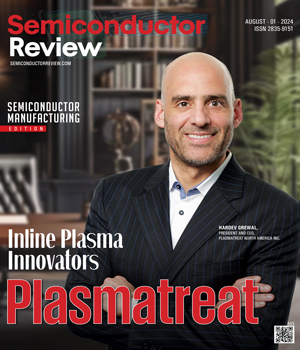
In this edition, we have featured Plasmatreat. The company’s Openair-Plasma® technology seamlessly lends itself to an inline process. It perfectly slots into any manufacturer’s assembly line to facilitate atmospheric plasma treatment between steps, improving surface quality and eliminating uncertainties of cross-contamination and recontamination.